ASIC Information and Datasheets
Quick link to the most used datasheets:
This page contains datasheets and other related information on the different ASICs that have been developed in view of offering components for power distribution systems. All these ASICs have been designed and qualified for radaition tolerance at different levels, and are targeted at switching frequencies that allow the use of air-core inductors (typical inductance range: 100 to 460nH). The table below summarises some of the main characteristics of the ASICs that are either available already, or that are being developed. Note that the radiation specifications are the levels required for the targeted application, but the radiation tolerance of the components might in some cases exceed these specs.

Naming of ASICs families The first family, the FEAST2, was historically named from a combination of the initial letters of the circuit designers. The number 2 reflects a major change in the final version. The final name is eventually followed by another number (FEAST2.1 or 2.2) that indicates a minor change in the circuit's version.
When it appeared clear that the ASIC offer had to be expanded to include different components of customisable power distribution systems, it seemed appropriate to reflect the specificities of each family in their name. A coherent naming convention was hence introduced, that is compatible also with possible future expansions of the offer. The name of each familiy is composed as follows:
xPOLy_vz.#
where x indicates the converter topology ("b" for buck, "r" for resonant, "Lin" for linear), y the maximum input voltage rating, z the voltage rating of the technology used for the design, and # the version number. The "POL" stands for Point Of Load, function that is common to all families.
bPOL48V buck DCDC converters
A new converter stage has been introduced, from 48V to 12V. It is a converter that has been developed under the EP-WP5.2 R&D program. It is composed by a rad-hard controller designed at CERN (GaN Controller) and a power stage with a commercial GaN chipset from EPC (EPC2152) which has been characterized for radiation.
The GaN Controller is designed in the same 0.35um high voltage technology of FEAST2, whose production Fab is unfortunately closing in 2022. A big production of 30 wafers has ben started and 2022 for a total of around 30k dies. This was last order buy, so we cannot produce more GaN Controller ASICs in the future.
Main information is depicted in the following picture:

The preliminary datasheet of the GaN_controller with the module (bPOL48V) is avaibale here:
the datasheet of the EPC2152 is avaibale here:
bPOL12V buck DCDC converters
This family is an upgrade of the FEAST2 family to the Displacement-Damage (DD) tolerance specifications for HL-LHC tracker applications. Simulation data report a radiation environment in both the ATLAS and CMS strip tracker detectors limited to about 60 Mrad and 1e15 n/cm2 (see the respective technical reports). With the addition of reasonable safety factors, the radiation tolerance specifications for the converters in this application are 150 Mrad and 2e15 n/cm2. Of course, specifications for tolerance to Single Event Effects remain unchanged: absence of destructive events or resets, transients on the output voltage limited in duration (a few us) and amplitude (below 10%).
The above specifications forbid the use of the FEAST2 converters, since they fail for DD effects at integrated fluxes of about 6-8e14 n/cm2. This failure is due to the damage induced by displacement damage on the 80V PMOS transistors used in the on-chip voltage regulators (these provide the regulated 3.3V to the control circuitry and to the drivers of the power transistors). The FEAST2 design has hence been moved to a "twin" CMOS technology where the voltage rating is decreased from 80 to 25V. The p-channel LDMOS transistors in this technology, also rated at 25V Vds, ensure that the on-chip regulators remain functional up to 6e15 n/cm2. Because of this increase in its radiation tolerance, the resulting new family of converters was intitially called upFEAST (from "upgraded FEAST") before the introduction of a coherent nomenclature.
The final version of the ASIC, bPOL12V_v25.6.1, is in production. The circuit will be packaged in a QFN32 with a pinout very similar to the latest versions of FEAST2. The final datasheet is available here:
A very important parameter for the relibaility of the bPOL12V is the design of the PCB. Please find here the guidelines for the PCB design (by Pablo Antoszczuk)
main informations are summarized in the following picture
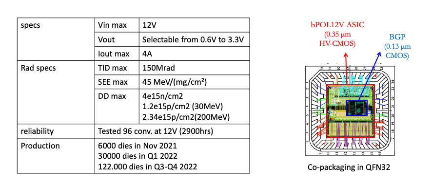
the previous version's datasheet, bPOL12V_v25.4, is avaiable here
bPOL2V5 buck DCDC converters
This component has been developed to allow for the construction of a multi-stage power distribution system, as illustrated in the image in the "Home" page. From an input voltage of 2.5V, provided from a first stage bPOL12V regulator, this converter can regulate an output voltage of 0.6 to 1.5V while providing a maximum output current of 3A.
The main information is depicted in the following picture
S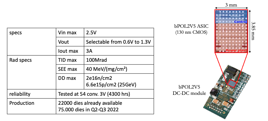
This circuit is designed in a 130nm CMOS technology, and uses the available I/O transistors to achieve the 2.5V input voltage compatibility. In the chosen technology, the I/O transistors offered as standard option have a nominal Vds rating of 2.5V (the v2 in the bPOL2V5 name stand for 2.5V rating). In a buck converter the current paths change several times during every switchin cycle: these large and rapid changes in the input (output) current to (from) the ASIC potentially determine large transients in the voltages seen by the ASIC. The amplitude of the transients is determined by the derivative of the current and the inductance along the current path. The nominal Vds of the I/O transistors is hence exceeded at every switching event, with potential detrimental effects on the reliability of the circuit. It is therefore critical to decrease the voltage transients to an acceptable level. This is done in the design by reducing the speed of the current switching, but this limitation affects the conversion efficiency. The other necessary provision is the reduction of the inductance along the current path. The required level of reduction is only possible by the adoption of a bump-bonding assembly technology AND a very careful PCB design, including the choice and placement of the passive components. This makes the integration of bPOL2V5 a delicate operation to be only done by experienced engineers/technicians who have to closely follow the provided guidelines (a recommended layout, together with additional indications, are available on request).
In order to increase the reliability of the bPOL2V5 famility we decided to move the design in a different flavour of the chosen 130nm CMOS technology with I/O transistors with a Vds rating of 3.3V. The use of these transistors would alleviate the stress imposed to the transistors during the current switching, and a prototype ASIC using this technology option has been designed and is being tested. The 3.3V transistors are considerably more affected by radiation, but the accurate design of the I/O part, taking into account the devices radiation degradation, was succesfull. The tests on the different prototypes indicate that the radiation tolerance specifications for strip tracker HL-LHC applications are met. The "v3" in the prototype name is a short form for the 3.3V transistor rating.
The production version, called bPOL2V5_v3.3 is today in stock. The final datasheet is available here
Datasheet of previous versions are available here (bPOL2V5_v2.2 and bPOL2V5_v3.2)
linPOL48V linear regulators
LinPOL48V is a linear regulator designed provide max Iout=200mA from Vinmax=48V. The defult Vout is fixed at 12V, but it can be tuned with an external voltage divider.
As for bPOL48V, linPOL48V is is designed in the same 0.35um high voltage technology of FEAST2, whose production Fab is unfortunately closing in 2022. A big production of 30 wafers has ben started and 2022 for a total of around 10k dies. This was last order buy, so we cannot produce more linPOL48V ASICs in the future.
The preliminary datasheet of the linPOL48V is avaibale here:
linPOL12V linear regulators
The linPOL12V family is born by a request from the ATLAS strip tracker groups, and based on the need to power a control circuit from the same (up to) 12V input voltage bus that supplies bPOL12V converters. In this scheme the control circuit needs to be powered independent on the enable/disable status of the bPOL12V, as illustrated in the scheme in the "Home" page. Since the current consumption of the control circuit is small (less than 80mA) and because of the need for a very small footprint, the natural choice for the power distribution component is a linear regulator.
This family uses the same technology as the bPOL12V familiy, and the regulators (there are two integrated in the same chip) use the same design developed for on-chip 3.3V regulation in the buck converter. In its standard configuration, the two voltage outputs regulate 1.4 and 3.3V respectively, but they can be changed with external components. The Datasheet is availbale here
Plese note that this chip has been designed and produced on a best effort basis and it has been agreed that the characterisation (electrical, radiation tolerance and reliability) was in the experiments hands. Both ATLAS and CMS are today running radiation tests in different facilities. When data will be available, they will be added to the datasheet.
DISCONTINUED: FEAST2 familiy of buck DCDC converters
FEAST2 ASIC is not anymore in production. the information are kept here for users that have used them in the past.
There is no possibility to buy anymore FEAST2 ASICs or wafers because the production fab is closed. This product is substitued by bPOL12V_V6.
This familiy of POL buck converters is suitable for use in radiation environments typical of the LHC or HL-LHC experiments, wherever the integrated flux of 1MeV equivalent neutrons is smaller than 5e14n/cm2. During the development of this circuit, different versions have been documented and provided to colleagues working on system integration. For historical reasons, the datasheet of all versions are still available for download, although at this time only FEAST2.1 circuits can be procured (soon replaced by FEAST2.2).
FEAST2.3 datasheet. Version 2.3 replaces 2.1 as production-ready ASIC in October 2018. It contains only a couple of small modifications rendering the chip more robust agains ESD events and against Total Ionising Dose (for the specific problem revealed in the CMS pixel system). This makes it suitable for applications in environments where the expected TID reaches or exceeds 500 krad (for doses below 500 krad, version 2.1 is adequate). - This datasheet is not available because it will not contain any modification with respect to version 2.1, since all functionalities are the same.
FEAST2.1 datasheet. FEAST2.1 is a revision of FEAST2 that has been designed at the beginning of 2015 in order to improve the yield of the circuit determined by failure of the PowerGood flag (that in a relatively important number of chips was stuck to 0). At the same time, a new feature has been introduced allowing for the monitoring of the T increase of the chip during operation via a dedicated analog signal (PTAT). This release replaces FEAST2 in all modules as from assembly runs in fall 2015.
FEAST2 ASIC datasheet. FEAST2 is the revision of FEAST that has been designed at the end of 2013 and manufactured at the beginning of 2014. The revision was justified by the wish to improve the radiation tolerance for SEEs, in particular to remove the resets in an hadron environment. This version was used in FEASTMP assemblies in 2014 and in the first part of 2015.
FEAST ASIC datasheet. FEAST was qualified in 2013 but still presented some sensitivity to SEEs (resets) that was improved in the next version. It has not been used in production modules.
AMIS2 ASIC datasheet. The AMIS2 converter is an early prototype that has been used in system tests rather widely. However, it integrates only the very basic functions of the final DCDC and is not really representative of the full converter ASIC